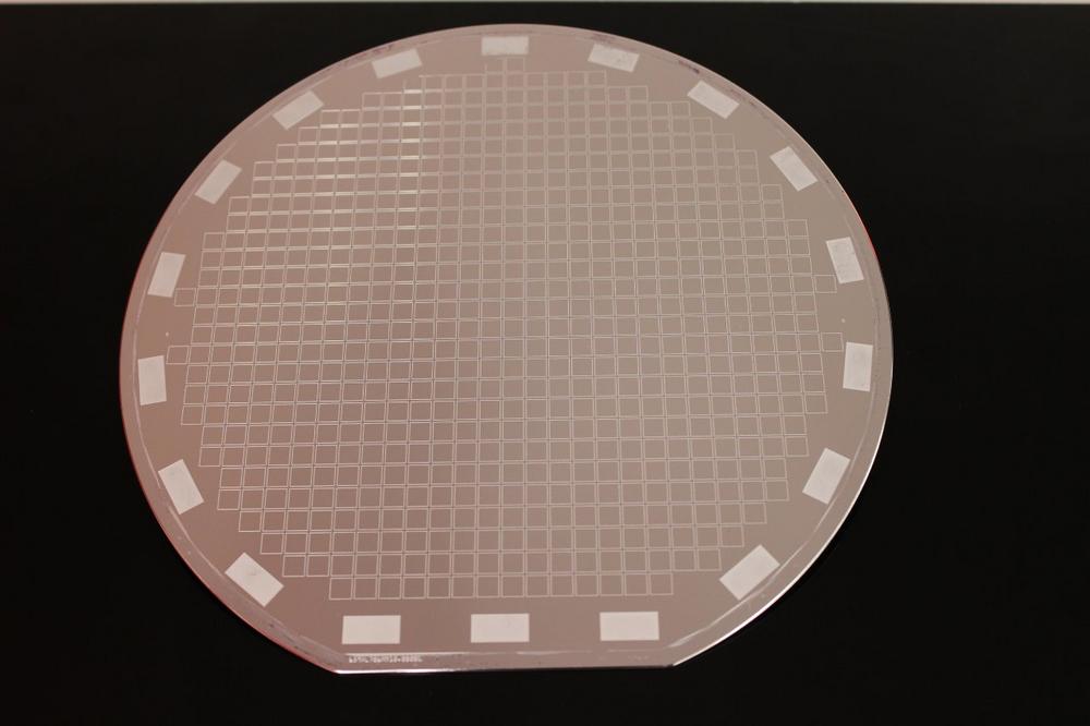
The patterning is done using pattern plating through a resist mask. After the deposition, the seed layer is etched and the patterns are electrically isolated. The layers can be used as conductor paths, heat management, bond pads or bond frames for chip and wafer-level bonding. The electrical properties of galvanically deposited aluminum correspond to those of bulk material to 87 percent. Thus, the properties of the electroplated aluminum are 10 percent better than those of aluminum layers deposited from the gas phase.
Further research and development work is focused on the long-term goal of using galvanic aluminum in both printed circuit board technology and semiconductor technology. Due to its material properties, aluminum is a good alternative to copper in printed circuit boards. In microsystems technology and microelectronics, aluminum is established as final metallization. A homogeneous material system would therefore be feasible with the help of ultrasonic flip chip assembly using aluminum pillars (instead of tin bumps).
The next steps will therefore address assembly and interconnection technology on aluminum surfaces and the coating of topographies, such as through-holes or blind holes, in the printed circuit board and on semiconductor substrates. The scaling of the process to 8-inch wafers or larger rectangular substrates is also being considered. To achieve this, a lot of engineering work has to be done in terms of plant technology in order to scale from laboratory equipment to industrial plants.
For the further development steps, the Fraunhofer ENAS is looking for interested companies, which are interested in a cooperation in the field of electroplated aluminium or just identified an application scenario for the electroplated aluminum. Furthermore, the deposition can be adapted as a service on customer-specific substrates with regard to size, material, seed layers, etc.
At the Fraunhofer joint booth in hall 5 (No. 248), Fraunhofer ENAS will present the process and possible applications of electroplated aluminum.
The Fraunhofer-Gesellschaft is the leading organization for applied research in Europe. Its research activities are conducted by 72 institutes and research units at locations throughout Germany. The Fraunhofer-Gesellschaft employs a staff of more than 26,600, who work with an annual research budget totaling 2.6 billion euros. Of this sum, 2.2 billion euros is generated through contract research. Around 70 percent of the Fraunhofer-Gesellschaft’s contract research revenue is derived from contracts with industry and from publicly financed research projects. International collaborations with excellent research partners and innovative companies around the world ensure direct access to regions of the greatest importance to present and future scientific progress and economic development.
Fraunhofer-Institut für Elektronische Nanosysteme ENAS
Technologie-Campus 3
09126 Chemnitz
Telefon: +49 (89) 1205-0
Telefax: +49 (89) 120575-31
http://www.enas.fraunhofer.de/
Marketing / PR
Telefon: +49 (371) 45001-204
Fax: +49 (371) 45001-304
E-Mail: andrea.messig-wetzel@enas.fraunhofer.de
Telefon: +49 (371) 45001-277
E-Mail: silvia.hertel@enas.fraunhofer.de
![]()
