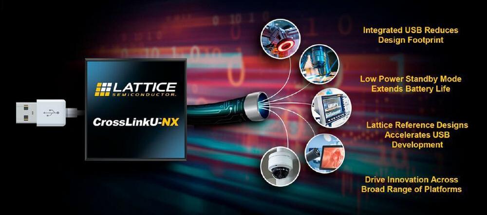
“Reducing power consumption, total cost of ownership, and design footprint are critical for expanding the potential of AI and vision applications,” said Dan Mansur, Vice President, Product Marketing, Lattice Semiconductor. “Lattice CrossLinkU-NX FPGAs are optimized to address these demands by integrating our low power, small form factor leadership with the popular USB connectivity interface to help designers extend battery life and simplify system design.”
Built on the award-winning Lattice Nexus™ platform, key features and performance highlights of the new low power Lattice CrossLinkU-NX FPGAs include:
Vision Processing FPGAs with USB
- Featuring hardened USB 2.0 up to 480 Mbps and USB 3.2 up to 5 Gbps
- Reducing total cost of ownership and area needed for discrete PHY components
- Reducing FPGA fabric resources required for USB device controller
Low Power Standby Mode with Always-On (AON)
- Extending battery life and simplifying system thermal management
- Optimizing power consumption in a typical embedded vision application
Complete Set of Reference Designs
- Offering a Lattice Propel™ template, host driver, and example host utilities for USB to I/O bridging and MIPI CSI-2 to USB bridging applications to accelerate USB device implementation on the FPGA
For more information about the technologies mentioned above, please visit:
- Lattice CrossLinkU-NX
- Lattice Nexus Platform
- Lattice Radiant Software
- Lattice Propel Design Environment
Availability and Pricing
CrossLinkU-NX FPGAs are sampling today and are supported by the latest release of Lattice Radiant® design software.
Information availability and pricing please visit email: sales.europe@macnica.com.
About Lattice Semiconductor
Lattice Semiconductor (NASDAQ: LSCC) is the low power programmable leader. We solve customer problems across the network, from the Edge to the Cloud, in the growing Communications, Computing, Industrial, Automotive, and Consumer markets. Our technology, long-standing relationships, and commitment to world-class support let our customers quickly and easily unleash their innovation to create a smart, secure, and connected world.
For more information about Lattice, please visit https://www.latticesemi.com/en. You can also follow us via LinkedIn, Twitter, Facebook, YouTube, WeChat or Weibo.
Lattice Semiconductor Corporation, Lattice Semiconductor (& design), and specific product designations are either registered trademarks or trademarks of Lattice Semiconductor Corporation or its subsidiaries in the United States and/or other countries. The use of the word “partner” does not imply a legal partnership between Lattice and any other entity.
GENERAL NOTICE: Other product names used in this publication are for identification purposes only and may be trademarks of their respective holders.
Founded in 1990 as ATD Electronique, Macnica ATD Europe headquarter offers in-novative components dedicated to imaging applications for the European market. Its product portfolio includes: image sensors (CCD, CMOS, InGaAs, Thermal etc.), op-tics, interface circuits, FPGA & IPs, imaging processors, cables and OLED micro-displays.
It also covers development tools and design services enabling fast and efficient reali-zation of new high-performance camera systems for markets such as machine vision, medical, life sciences, surveillance, automotive and others. After the acquisition of the company by Macnica Inc. as of October 1, 2020 the company operates under the name Macnica ATD Europe.
About Macnica ATD Europe GmbH, (former Macnica GmbH)
Macnica’s ATD Europe GmbH, (former Macnica GmbH), was originally established in the UK in 2006, and moved to Germany in July 2008, to increase efficacy of its service for European customers.
By it’s acquisition of the Munich based company Scantec Mikroelektronik in 2014 Macnica Europe formed a powerful semiconductor distribution with headquarter in Ingolstadt and offices in Munich, Regensburg, Milton Keynes (UK) and Warsaw of-fering an attractive and competitive portfolio of highly sophisticated devices.
Macnica provides end to end support from design-in to production through its global service network to its customers, regardless of the final destination of the product shipment to customers’ manufacturing locations.
About Macnica, Inc.
Macnica was established in 1972 as a semiconductor distribution company headquar-tered in Yokohama, Japan, and has over 85 sales offices worldwide in eastern Asia, Europe and the USA. Total number of employees is over 3,900 and its consolidated revenue for fiscal 2021 was approximately US$ 7.6 B.
Macnica is famous for having an excellent engineering team of more than 900 appli-cation support engineers, IC designers and software developers with strong focus on providing technical support for its customers including custom design services. Mac-nica is continuing to extend its presence globally by having successful partners in strategic areas in the electronics market.
Macnica ATD Europe GmbH
Nürnberger Str. 34
85055 Ingolstadt
Telefon: +49 (841) 88198-0
Telefax: +49 (841) 88198199
http://www.macnica.eu/de
Marketing
Telefon: +49 (89) 899143-15
Fax: +49 (89) 899143-17
E-Mail: josef.sigl@macnica.com
Telefon: +49 (841) 88198-102
E-Mail: sales.europe@macnica.com
![]()
